Along with some brand-new statements for their 2nm procedure node strategies, TSMC has actually likewise launched a development and roadmap upgrade for their N3 household procedure innovations at today’s 2023 North American Innovation Seminar. TSMC’s last generation of FinFET-based procedure nodes, the N3 household is anticipated to stay around in some shape or kind for several years to come as the densest node offered for clients who do not require a more advanced GAAFET-based procedure.
TSMC’s huge roadmap updates on the N3 front were with N3P and its high efficiency version, N3X. As exposed today by TSMC, N3P will be an optical diminish of N3E, offering boosted efficiency, decreased power usage, and increased transistor density compared to N3E, all while preserving compatibility with N3E’s style guidelines. On the other hand, N3X will wed severe efficiency with 3nm-class densities, using greater clockspeeds for high efficiency CPUs and other processors.
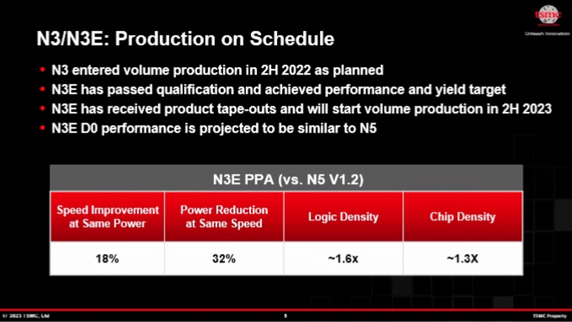
N3E: 3nm for Everybody Is on Set Up
As a fast refresher, TSMC’s N3 (3nm-class) household of procedure innovations is consisted of a number of variations, consisting of standard N3 (aka N3B), unwinded N3E with decreased expenses, N3P with boosted efficiency and chip density, and N3X with greater voltage tolerances. In 2015 the business likewise spoke about N3S with made the most of transistor density, however this year the business stays tight lipped about this node and it is not pointed out throughout its slides.
TSMC’s vanilla N3 node includes as much as 25 EUV layers (according to China Renaissance and SemiAnalysis), with TSMC utilizing EUV double-patterning on a few of them to produce greater reasoning and SRAM transistor density than N5. EUV actions are costly in basic, and EUV double pattern drives those expenses up even more, which is why this fabrication procedure is just anticipated to be utilized by a handful of clients who are not as worried about the high expense needed.
| Marketed PPA Improvements of New Process Technologies . Information revealed throughout teleconference, occasions, press rundowns and press releases |
|||
| TSMC | |||
| N3 . vs . N5 |
N3E . vs . N5 |
||
| Power | -25 -30% | -32% | |
| Efficiency | +10 -15% | +18% | |
| Reasoning Location(* )Decrease *%
Reasoning Density * . |
-42%
1.7 x . |
-37.5%(* )1.6 x
. . |
|
| 0.0199 µm ² (-5 %vs N5) | . | . | |
| Late 2022 .(* )H2 2023 |
.(* )Most of TSMC’s customers thinking about a 3nm-class procedure are anticipated to utilize the | , which according to TSMC is on schedule and accomplishing their efficiency targets. N3E consumes to 19 EUV layers and does not count on EUV double pattern at all( according to information from | |
), lowering its intricacy and expenses. The compromise is that N3E uses lower reasoning density than N3, and it has the exact same SRAM cell size as TSMC’s N5 node, making it rather less appealing to those clients who are driving for density/area gains. In general, N3E assures a larger procedure window and much better yields, which are 2 important metrics in chip fabrication.(* )” N3E will be much better than N3 in regards to yield, procedure intricacy, which straight equating into (* )procedure window,” stated Kevin Zhang, Vice President of Organization Advancement at TSMC. N3P: Greater Efficiency, Greater Transistor Density Following N3E, TSMC will continue to enhance the N3 household’s transistor density with N3P, which will develop on N3E by using enhanced transistor attributes. The refined procedure node will enable chip designers to either boost efficiency by 5% at the exact same leak or lower power by 5% ~ 10% at the exact same clocks. The brand-new node will likewise increase transistor density by 4% for a ‘blended’ chip style, which TSMC specifies as a chip including 50% reasoning, 30% SRAM, and 20% analog circuits. As part of their conversation on N3P, TSMC worried that the density enhancement was attained by changing the optical efficiency of its scanners. So it is most likely that TSMC will have the ability to diminish all kinds of chip structures here, which will make N3P an appealing node for SRAM-intensive styles.” N3P is an efficiency increase, it has a 5% greater efficiency, a minimum of a 5% greater than N3E,” described Zhang. It likewise has the 2% optical diminish, which bring transistor density to 1.04 x.”
.
[wider]
.
.
Marketed PPA Improvements of New Process Technologies
. Information revealed throughout teleconference, occasions, press rundowns and news release .
.
|
TSMC . . |
|||||
|
. N5 |
N3E | ||||
|
N3P . vs . N3E |
N3X . vs . N3P |
. . Power |
-25 -30% . -32% |
||
| greater | . | Efficiency | +10 -15% | +18 % | |
| . | . | . | . |
. 1.04 x(* ) . exact same |
|
| . | . | . (* )? | . | . | |
| Late 2022 | . | . | Given That N3P is an optical diminish of N3E, it will protect N3E’s style guidelines, allowing chip designers to rapidly recycle N3E IP on the brand-new node. Subsequently, N3P is likewise forecasted to be among TSMC’s most popular N3 nodes, so anticipate IP style homes like Cadence and Synopsys to provide a range of IP for this procedure innovation, profiting of forward compatibility with existing N3E at the same time. TSMC states that N3P will be production prepared in the 2nd half of 2024. | Lastly, for designers of high-performance computing applications like CPUs and GPUs, TSMC has for the previous couple of generations been using its X household of high voltage, performance-focused nodes. As divulged at last year’s occasion, the N3 household will be getting its own X version with the appropriately called N3X node. | |
| The last N3 household node in TSMC’s present roadmap, the business states that that N3X will be production prepared in 2025.
| |||||